MyArcade Cabinet Customization: Difference between revisions
(→Understanding the ASIC startup: SPI information) |
m (→Understanding the ASIC startup: Changes to SPI protocol) |
||
| Line 251: | Line 251: | ||
You can understand a little more about SPI at [https://www.analog.com/en/analog-dialogue/articles/introduction-to-spi-interface.html Analog's website]. A basic introduction sufficient to understand this cabinet can be had below. | You can understand a little more about SPI at [https://www.analog.com/en/analog-dialogue/articles/introduction-to-spi-interface.html Analog's website]. A basic introduction sufficient to understand this cabinet can be had below. | ||
SCLK clocks data in/out of the chip. The U6 ASIC will first send a command, such as "Read Block" on SI and then the blocks data will be read out on SO. These data in/out will be "Single SPI", so although the command might be a single byte such as 0xE7 the SI pin will be clocked 8 times in serial with each bit. | |||
See the "Applications" section at the bottom of this article for a Tektronix TLA listing file decoder used in the live sniffing of EEPROM data. | |||
[[File:018.MyArcade.SPI Reading.jpg|alt=SPI Reading|none|thumb|SPI Reading]] | |||
- MOSI, multi-drop << WAVEFORM and wiring >> | - MOSI, multi-drop << WAVEFORM and wiring >> | ||
| Line 259: | Line 261: | ||
- Reason for decoder in python is size of data likely to be seen; not trying to make generic SPI but specific reader | - Reason for decoder in python is size of data likely to be seen; not trying to make generic SPI but specific reader | ||
<WAVEFORM PICTURE> | <WAVEFORM PICTURE> | ||
Revision as of 09:43, 1 March 2023
General introduction
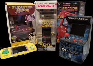
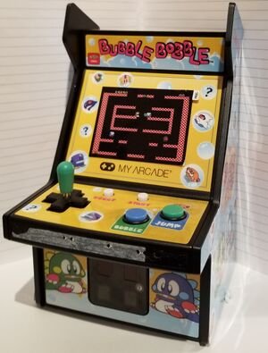
The DreamGear, now rebranded MyArcade, micro-player/mini-arcade/etc cabinets are a collection of NES game emulator toys. See The MyArcade Gaming web site where you can buy direct, or also via Amazon
There are a number of MyArcade cabinets, the micro player only play a single title and the mini player play multiple-titles. At time of writing there were 14 different micro player cabinets which all boot to one game only, and two mini player cabinets which boot many titles from namco, or data east.
In reality some contain only one game title whilst others contain many but the power-on game title is determined by make/break pads inside the cabinet PCB.
These units also have a interchangeable no-button, one-button, and two-button game pad tray. This tray can be popped out with a little pressure.
Opening the Cabinet
This section deals with getting into the cabinet.
Opening main cabinet unit
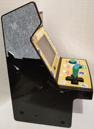
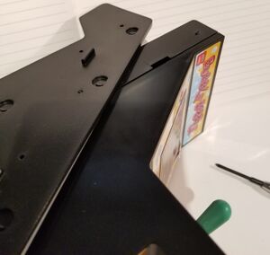
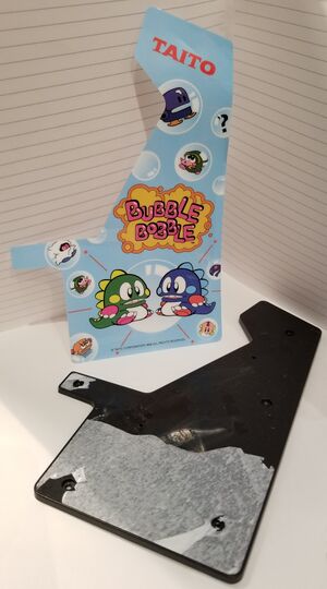
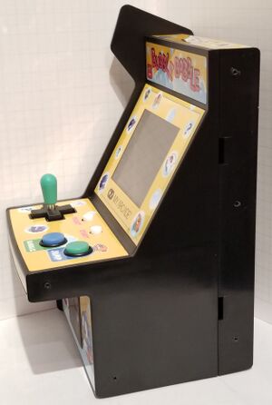
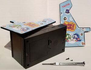
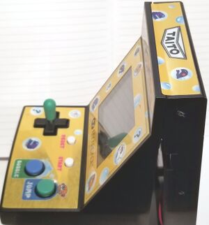
The cabinet has stickers on the left and right which conceal screws that hold on these thick side panels. These stickers are best removed with a heat gun, Exacto blade down the seam, or alternatively puncture the screw heads and unscrew. I didn't care so just ripped them off which bent them meaning they were hard to place back neatly.
 |
 |
 |
 |
 |
 |
 |
Now you have the case open you need to disconnect the internal PCBs in order to get at the main board. To do this you will need to remove the "USB power port / power/ speaker" distribution panel screwed into the back of the cabinet case. This needs removing by unscrewing the two retaining screws.
Then to get at the main board front you will need to pop the mainboard off, and to make things easier also the power button at the bottom.
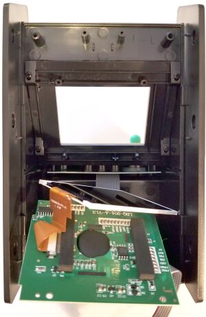
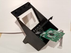
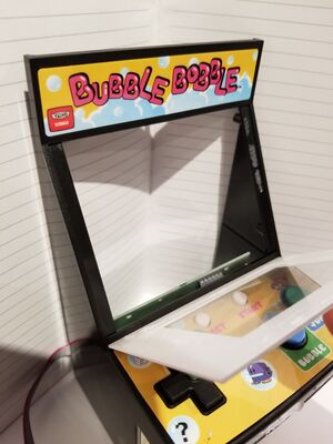
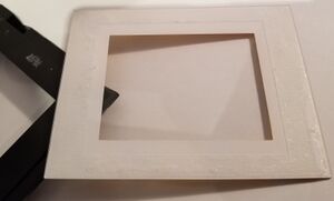
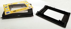
Once you do this the display is then held in place by a plastic housing and rubber pads to the front plastic cover which is held on by screws and the outer cabinet sticker - so it will just drop out.
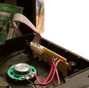 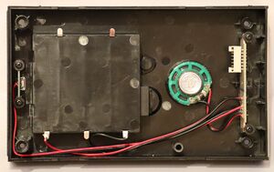 |
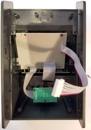 |
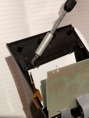 |
 |
 |
   |
Removing the Joypad
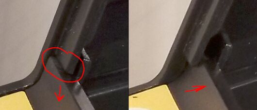
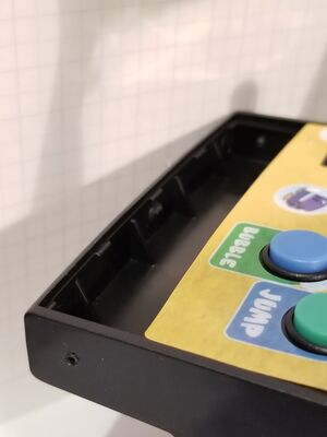
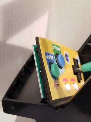
The last remaining PCB is the button panel, which is not necessary and a little harder to remove.
 | |
 |
 |
Final disassembly view
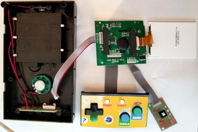
Here is what it looks like after complete removal. The back plate has the speaker heat-melted into place, with the audio jack at the top with the volume buttons and the USB-power PCB at the bottom that run over the ribbon cable to the main board PCB. The main board then has a LCD connector, power button/LED PCB, and joypad draw PCB.
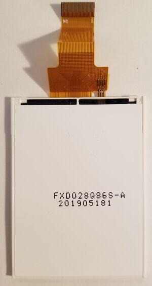
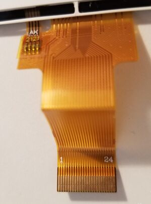
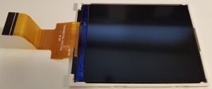
LCD Views
d
 |
 |
 | |
PCB Views
x
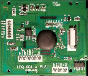 |
|
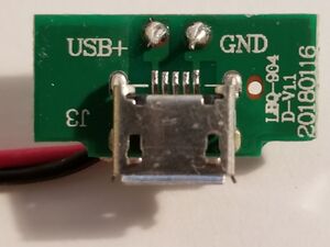 |
|
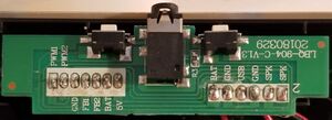 |
Main Circuit board
The main board consists of an emulator chip-on-board ( aka Chip-On-Board or Glob/Blob-top ) , SPI flash chip of 8Mbits (1Mbyte), a PWM speaker driver, and an unknown ASIC.
| Silk Screen ID | Chip Designation | Description |
|---|---|---|
| U6 | chip-on-board ASIC | NES Emulator Chip |
| U2 | SC662K-3.3V | 3.3V LDO |
| U3 | GD25Q80C / XT25F08B | 8Mbit SPI Flash |
| Q1 | S8550 PNP (2TY) | |
| U7 | NO-MARKING | PWM FB1/FB2 back buttons |
| U8 | ST3157 | PWM SOUND Switch |
The chip-on-board ASIC, is something like the VT03, which is a complete NES emulator. It includes a 6502 CPU, PPU Graphic Unit with LCD output, SPU Sound Unit, two internal 2KBytes SRAMs, SPI, and some General Purpose I/O controller. It also contains a unique mapper that allows for mapping up to 1MB, maybe more into the small 65KB memory space.
The GPIO comes out to the various joystick and game buttons. Whilst the SPI is used to house various games that are mapped into the 6502 CPU's upper memory region $8000-$FFFF. By selecting the mapping address its possible to load any number of games from the flash.
<mapping graphic>
Main PCB SPI EEPROM
The SPI EEPROM can be a number of different types but is somewhere up to an 8Mbit SPI flash EEPROM. For the single-game cabinets there is a lighter "startup routine", for the multi-title cabinets (and some of the single title cabinets) the IOB are read by the initial "startup routine" and a table the SPI EEPROM is read and a new program (the game) is mapped and started.
All cabinets map the SPI EEPROM 0x7_B000~0x7_FFFF into the m6502 CPU's memory at address XXXX ~ 0xFFFF with the m6502 resetting and running the instruction from 0xFFFC~0xFFFF.
IOB in Mappy Cabinet
IOB mapping on some of the Cabinets will read the ROM table if there are multiple titles and boot that title instead.
MSB... LSB
   IOB2 -- furthest from U3 chip
   IOB3
   IOB1 -- closest to U3 chip (overlap to legs area)

    000 - Rolling Thunder
    001 - PacMan
    010 - Galaga
    011 - Galaxian
    100 - Mappy
    101 - DigDug
    110 - Mappy
    111 - Rolling Thunder
Below is the picture of the area of IOB near the main ASIC U6, and next to U3 ASIC.
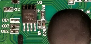
Dumping the ROM
The SPI ROM cannot have a programmer attached, and the ROM must be disconnected from the +V rail in order to run or boot. Cutting the track and inserting a switch to toggle on the 5V rail works.
| Model | SPI ROM Part # | ROM SHA256 | Games Contained |
|---|---|---|---|
| Mappy | XT25F08B | d0a9ae89205fa078564a4fd6dc778cdcfc045386755e549f1110d7f5b5b4bf02 | Mappy, Pacman, Rolling Thunder, Galaga, Galaxian |
| Bubble Bobble | GD25Q08C-SIG (Datasheet) | 0136a88ae8a7bee3a2cbcc196a33a4c284291be18050debb90fa73faef740f5a | Bubble Bobble |
Useful for checking NES images are the CHR rom editors such as NES Sprite Editor. The CHR ROM are hard to spot visually but do have a tendency to contain 00s and "3" characters because of the way the planar data is recorded
A deeper discussion for graphics can be seen at DustMop.io
The TILE and SQUARE mapping can be seen NES FAQ
Understanding the ASIC startup
The following sections deal with understanding how the cabinet goes from power on, thru CPU reset, initial startup routine, and then game start along with multi-page (multi-rom) games and how mapping is done.
SPI EEPROM
SPI EEPROMs use the SPI bus as a single bit bus with clocking allowing for simple interface for access to mass amounts of storage. The SPI EEPROM appears to only use "Standard SPI" where SO/SI are used, but SPI EEPROMS are capable of doing Dual (2bit using DQ0/DQ1) and Quad (4 bit using DQ0/1/2/3) SPI for faster bulk data IO.
General package used in the cabinets looks like below
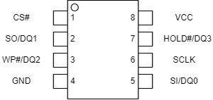
The meaning of each pin can be understood as below.
| Pin # | Pin Name | In/Out | Description |
|---|---|---|---|
| 1 | CS# | In | Chip Select; Active when Low, must NOT be left floating |
| 2 | SO/DQ1 | In/Out | Data Ouput / Data In-Out bit 1 |
| 3 | WP#/DQ2 | In/In-Out | Write Protect Input / Data In-Out bit 2 |
| 4 | GND | Ground pin | |
| 5 | SI/DQ0 | In/In-Out | Data Input / Data In-Out bit 0 |
| 6 | SCLK | In | Serial Clock In |
| 7 | HOLD#/DQ3 | In/In-Out | Hold Input; Active when Low / Data In-Out bit 3 |
| 8 | VCC | Power Supply Pin |
Monitoring SPI Bus
You can understand a little more about SPI at Analog's website. A basic introduction sufficient to understand this cabinet can be had below.
SCLK clocks data in/out of the chip. The U6 ASIC will first send a command, such as "Read Block" on SI and then the blocks data will be read out on SO. These data in/out will be "Single SPI", so although the command might be a single byte such as 0xE7 the SI pin will be clocked 8 times in serial with each bit. See the "Applications" section at the bottom of this article for a Tektronix TLA listing file decoder used in the live sniffing of EEPROM data.
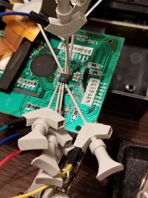
- MOSI, multi-drop << WAVEFORM and wiring >>
- QUAD mode << WAVEFORM inc. E7h command >>
- Reason for decoder in python is size of data likely to be seen; not trying to make generic SPI but specific reader
<WAVEFORM PICTURE>
- 100MHZ? FIXME
- sample E7h command + continuous read mode
NOTES;
- Multiple accesses to same memory location, appears to have zero caching
- Other random low-memory accesses to 0x0000 - 0x1FFF
- Accesses are WORD aligned so access to read 0x00F1 means 0x00F0 gets read, then 0x00F2
Decoding the SPI for a simple boot session can look like the following, part way through.
 line# 14110198 READ:* 0x7effe(mode=0xa5): 0xf120
 line# 14110212 READ:* 0x7effe(mode=0xa5): 0xf120
 line# 14110226 READ:* 0x7effe(mode=0xa5): 0xf120
 line# 14110240 READ:* 0x7f000(mode=0xa5): 0x0df1
 line# 14110254 READ:* 0x7f000(mode=0xa5): 0x0df1
 line# 14110268 READ:* 0x7f000(mode=0xa5): 0x0df1
 line# 14110282 READ:* 0x7f000(mode=0xa5): 0x0df1
 line# 14110296 READ:* 0x7f000(mode=0xa5): 0x0df1
 line# 14110310 READ:* 0x7f000(mode=0xa5): 0x0df1
 line# 14110408 READ:* 0x7f10c(mode=0xa5): 0x608a
 line# 14110422 READ:* 0x7f10c(mode=0xa5): 0x608a
 line# 14110436 READ:* 0x7f10c(mode=0xa5): 0x608a
This fits perfectly with the ROM disassembly for this memory location, assuming 0x7_E000 is mapped to m6502 CPU memory at 0xE000.
ROM:EFF4 09 04                                   ORA     #4
ROM:EFF6 8D 4B 41                                STA     byte_414B
ROM:EFF9 20 0D F1                                JSR     xsub_F10D_Delay
ROM:EFFC 20 0D F1                                JSR     xsub_F10D_Delay
ROM:EFFF 20 0D F1                                JSR     xsub_F10D_Delay <--- here
ROM:F002 20 0D F1                                JSR     xsub_F10D_Delay
ROM:F005 20 0D F1                                JSR     xsub_F10D_Delay
ROM:F008 60                                      RTS
ROM:F008                         ; End of function xsub_EF83_CART_DoSomething

ROM:F10C 60                                      RTS
ROM:F10D                         xsub_F10D_Delay:
ROM:F10D 8A                                      TXA
The above method was very useful in working out that the System-Test feature used 0x6_3000 for its CHR memory.
SPI 1MB Flash layout
The cabinet starts up with at first accesses to SPI at 0x1000, repeating until around XXXms. This then starts the MOS 6502 which defaults to SPI address 0x7_XXXX. The MOS 6502 RESET vector can be seen as the first read at SPI address 0x7_FFFC and then of course instruction reads happen from the address read from 0x7_FFFC.
The code at 0x7_XXXX ~ 0x7_FFFF is a custom NES Emulator ASIC initialization routine setting various custom values.
- In the case of the bubble bobble cabinet, it copies code to low RAM and this remaps the SPI to 0x?_???? then jumps to that ROM reset vector starting Bubble Bobble
- In the case of the Mappy/XX/YY/ZZ cabinet, it reads IOB pad values, copies code to low RAM which maps 1-of-6 titles, and this remaps the SPI to 0x?_???? then jumps to that ROM reset vector starting Bubble Bobble
Bubble Bobble Cabinet ROM
0_0000 PRG: Bubble Bobble Game

7_B000 Game Entry Table

7_C000 Initial Reset Handler Code
Mappy Cabinet ROM
0_0000 PRG: "BANK0" string, per Rolling Thunder	 	(ROLLING THUNDER : 8000-9FFF)
0_2000 PRG:                              		 	(ROLLING THUNDER : A000-BFFF)

0_4000 ???:                              			(ROLLING THUNDER : [ Title Screen texts here ] )
0_8000 ???: "BANK2" string, per Rolling Thunder		...
0_A000 ???: More data								...
0_C000 ???: "BANK3" string, per Rolling Thunder		...
0_E000 ???: More data
1_0000 ???: More data
1_2000 ???: More data
1_4000 ???: More data
1_6000 ???: More data
1_8000 ???: More data
1_A000 ???: More data								...
1_A000 ???: More data								(ROLLING THUNDER : Unknown data)

1_C000 PRG: ROLLING THUNDER (B000-DFFF)
1_E000 PRG: ROLLING THUNDER (E000-FFFF)

2_0000 CHR: Rolling Thunder
2_2000 CHR: Rolling Thunder
2_4000 CHR: Rolling Thunder
2_6000 CHR: Rolling Thunder
2_8000 CHR: Rolling Thunder
2_A000 CHR: Rolling Thunder
2_C000 CHR: Rolling Thunder
2_E000 CHR: Rolling Thunder
3_0000 CHR: Rolling Thunder
3_2000 CHR: Rolling Thunder
3_4000 CHR: Rolling Thunder
3_6000 CHR: Rolling Thunder
3_8000 CHR: Rolling Thunder
3_A000 CHR: Rolling Thunder
3_C000 CHR: Rolling Thunder
3_E000 CHR: Rolling Thunder

4_0000 PRG: PACMAN
4_2000 PRG: PACMAN
4_4000 CHR: PACMAN

4_6000 CHR: MAPPY
4_8000 PRG: MAPPY
4_A000 PRG: MAPPY

4_C000 PRG: DIGDUG
4_E000 PRG: DIGDUG
5_0000 CHR: DIGDUG

5_2000 CHR: GALAGA
5_4000 PRG: GALAGA?????
5_6000 PRG: GALAGA?????

5_8000 PRG: GALAXIAN
5_A000 PRG: GALAXIAN
5_C000 CHR: GALAXIAN  (Weird: Contains strings "MISSION" "DESTROY" "CONVOY" "CHARGER" "READY" "PAUSE" "START" "GALAXIA" )

5_E000 FF..FF..FF..
6_0000 CHR: "4in1" / "PAC-MAN" / "FROGGER" / ???? title names
6_2000 CHR: "4in1" and "380in1" / FONTS / ASTEROID / QBERT / PAC-MAN / ICONS for Qbert/PAC-MAN
6_4000 CHR: "GAMES LIST" / "ENGLiSH/JAPANESE"

7_0000 PRG:  Not sure what this applicaiton is, but its a program; mapped to 0x8000
7_2000 ???:	 Not sure (Up to 7_54D0)

7_5800 ???:  Some data

7_A000 ???:  Some table
7_A400 ???:  Some other table


7_B000 Game Image Mapper Table (See below)

7_C000 Inital boot rom
			00: 06 <number of games in cabinet> ....
			10: ZERO terminated list of game names

7_F000 Initial boot rom (exec at 7_FFFC as reset vector)

8_0000 FF FF ...
F_FFFF FF FF
Mapping NES Cartridge to SPI Memory
If the ROM is 1 page then it maps to 0xF000, if its two then 0xE000, and so on until 0x8000.
After this the FIRST two pages map to 0x8000 and 0xA0000 respectfully, and the LAST two pages map to
0xC000, and 0xE000
<< Rollercoster thingy ROM example >>
<< PICTURE side by side .... >>
 * NES expects
 *    0x8000 = PAGE0 : Your Code
 *    0xA000 = PAGE1 : Your Code
 *    0xC000 = PAGE2 : Your Code
 *    0xE000 = PAGE3 : Code + Reset Vectors
 *      0xFFF4 COP
 *      0xFFF6 N/A
 *      0xFFF8 ABORT
 *      0xFFFA NMI
 *      0xFFFC RESET
 *      0xFFFE IRQ/BRK
Controlling the Mapping
Discussion of the MMC, best left to the NESDEV wiki however the
and then discussion of the table at 7_B000.
At reset the ASIC mapps 0x8000-0xAFFF to RAM.
And 0xB000-0xFFFF to SPI Flash at 7_B000-7_FFFF.
In the Mappy/Pacman/Digdug/Galaga/Galaxian/Rolling Thunder cabinet
this section is a rom switcher. It will setup the ASIC correctly,
then will jump to the right game based on IOB shorting.
In BubbleBobble its just a system setup program, and will only jump to the game.
All cabinets also support UP-JOY + SELECT for a test mode.
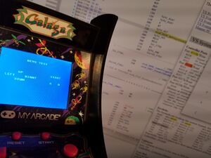
IOB are read ($4147??) and this is used to select entry from table.
These are loaded into the MMC and the system is restarted.
M6502 CPU Code Analysis
Initial Reset Code, and Game Table Format
At reset the 0x7_B000 ~ 0x7_FFFF is mapped into the m6502 memory space and the RESET vector is taken. The Mappy and bubble bobble cabinet have similar reset handler code. It looks at the IOB values, uses this with a Game Table at 0x7_B000 to program the mapper and then boot that mapped game cartridge code.
The values from the Game Table are 9 bytes long and represent mapper registers that will be loaded for that game.
Example Table Entry
	ROM TABLE $B000
		ROM:B000 00       .BYTE   0               ; CHR Bank MSB; Always 0
		ROM:B001 00       .BYTE   0               ; CHR Bank Mid; 0 / $10 / $20
		ROM:B002 81       .BYTE $81               ; CHR Bank LSB;
		ROM:B003 02       .BYTE   2               ; MMC mapper (2,4: Four ROM Banks or 5: Two Rom Banks )
		ROM:B004 00       .BYTE   0               ; PRG Bank0 x 2
		ROM:B005 01       .BYTE   1               ; PRG Bank1 x 2
		ROM:B006 0E       .BYTE  $E               ; PRG Bank2 x 2
		ROM:B007 0F       .BYTE  $F               ; PRG Bank3 x 2
		ROM:B008 00       .BYTE   0               ; Mirrored / Vertical - A000h


All Entries for Mappy Cabinet

	RT ROM:B000 00 00 81 02 00 01 0E 0F+                struc_RomTable <0, $00, $81 20 10, 2, $00, $01, $0E, $0F, 0>
	PM ROM:B009 00 00 10 16 05 20 21 20+                struc_RomTable <0, $10, $16  5  2, 5, $20, $21, $20, $21, 1>
	MA ROM:B012 21 01 00 10 1E 05 24 25+                struc_RomTable <0, $10, $1E  7  3, 5, $24, $25, $24, $25, 0>
	DD ROM:B01B 24 25 00 00 10 46 05 26+                struc_RomTable <0, $10, $46 11  8, 5, $26, $27, $26, $27, 1>
	GL ROM:B024 27 26 27 01 00 10 4E 05+                struc_RomTable <0, $10, $4E 13  9, 5, $2A, $2B, $2A, $2B, 1>
	GA ROM:B02D 2A 2B 2A 2B 01 00 10 76+                struc_RomTable <0, $10, $76 1D  E, 5, $2C, $2D, $2C, $2D, 1>
So calculating the CHR/PRG mapping for the Mappy cabinet looks something like the following
	Case ($201A & 0x07) => Video Mode and affects MASK value.
		 Normal Video Modes:   ($4100&0x0F)<<21+($2018&0x70)<<14+(($201A&0xF8)|(VBANK&0x07))<<10
		 Enhanced Video Modes: ($4100&0x0F)<<21+(($201A&0xF8&MASK)|(VBANK&0x07))<<13+EVA<<10
									76543210
	ROLLING  CHR> 2_0000		81	10000001	10000 001	10	1	0x10 * 0x2000 -> 2_0000
	PACMAN   CHR> 4_4000		16	00010110	00010 110	 2	6	0x02 * 0x2000 -> 0_4000
	MAPPY    CHR> 4_6000		1E  00011110	00011 110	 3	6	0x03 * 0x2000 -> 0_6000
	DigDug   CHR> 5_0000		46  01000110	01000 110	 8	6	0x08 * 0x2000 -> 1_0000
	GALAGA   CHR> 5_2000		4E  01001110	01001 110	 9	6	0x09 * 0x2000 -> 1_2000
	GALAXIAN CHR> 5_C000 		76  01110110	01110 110	 E	6	0x0E * 0x2000 -> 1_C000
MyArcade Custom Mapper Registers
   $4100,  Program Bank1, Video Bank2                   PA[24:21]VA[24:21]
   $2018,  Video Bank1 register, BKPAGE, Video RW Bank  X|VA[20:18]|BKPAGE|VRWB[2:0]
			Write $00/10/20 ( Intermediate CHR Bank number; PPU $0000-$1FFF: Selected by register $2018 bits 4-6 (VA18-20). )
   $201A,  Video Bank0 register6, Video Bank0 selector  RV6[7:3]VB0S[2:0]
   $410B,  MMC mapper (2,4: Four ROM Banks or 5: Two Rom Banks )
   $4107,  PRG ROM Bank0: $8000 or $8000
   $4108,  PRG ROM Bank1: $A000 .. $C000
   $4109,  PRG ROM Bank2: $C000    $8000
   $410A,  PRG ROM Bank3: $E000    $C000
   $A000
MyArcade Custom Register Map
    $2010/2011  / 2018

    $4105    SEEN: Bubblebobble
    $410B    SEEN: Bubblebobble

    $4144    SEEN: Bubblebobble
    $4146    SEEN: Bubblebobble

    $4147,  IOB/GPIO

    $4148    SEEN: Bubblebobble
    $414A    SEEN: Bubblebobble
    $414C    SEEN: Bubblebobble
    $414E    SEEN: Bubblebobble

    $414F    SEEN: Bubblebobble

    $4155    SEEN: Bubblebobble
    $4157    SEEN: Bubblebobble
    $415A    SEEN: Bubblebobble
    $415B    SEEN: Bubblebobble

    $41E4    SEEN: Bubblebobble
    $41E6    SEEN: Bubblebobble
    $41E8    SEEN: Bubblebobble

https://problemkaputt.de/everynes.htm#mapper4mmc3prg8kvrom2k1kntsramirq
    $8000 / 8001 :
Applications and Tools
Hex Dump NES Application : https://github.com/lucienmp-nes/NesHexDumpTool
Tektronix TLA SPI EEPROM Listing file to data decoder : https://github.com/lucienmp-nes/TLAWaveformParser
Other Cabinet stuff
* https://wrongbaud.github.io/MK-Teardown/
* https://boards.dingoonity.org/other-game-systems/identify-myarcade-pacman-pocket-player-hardware/
RANDOM LINKS
Very close to the "Mapper 64: Tengen RAMBO-1 - PRG/8K, VROM/2K/1K, NT, IRQ"
Or : Mapper 4: MMC3 - PRG/8K, VROM/2K/1K, NT, SRAM, IRQ
